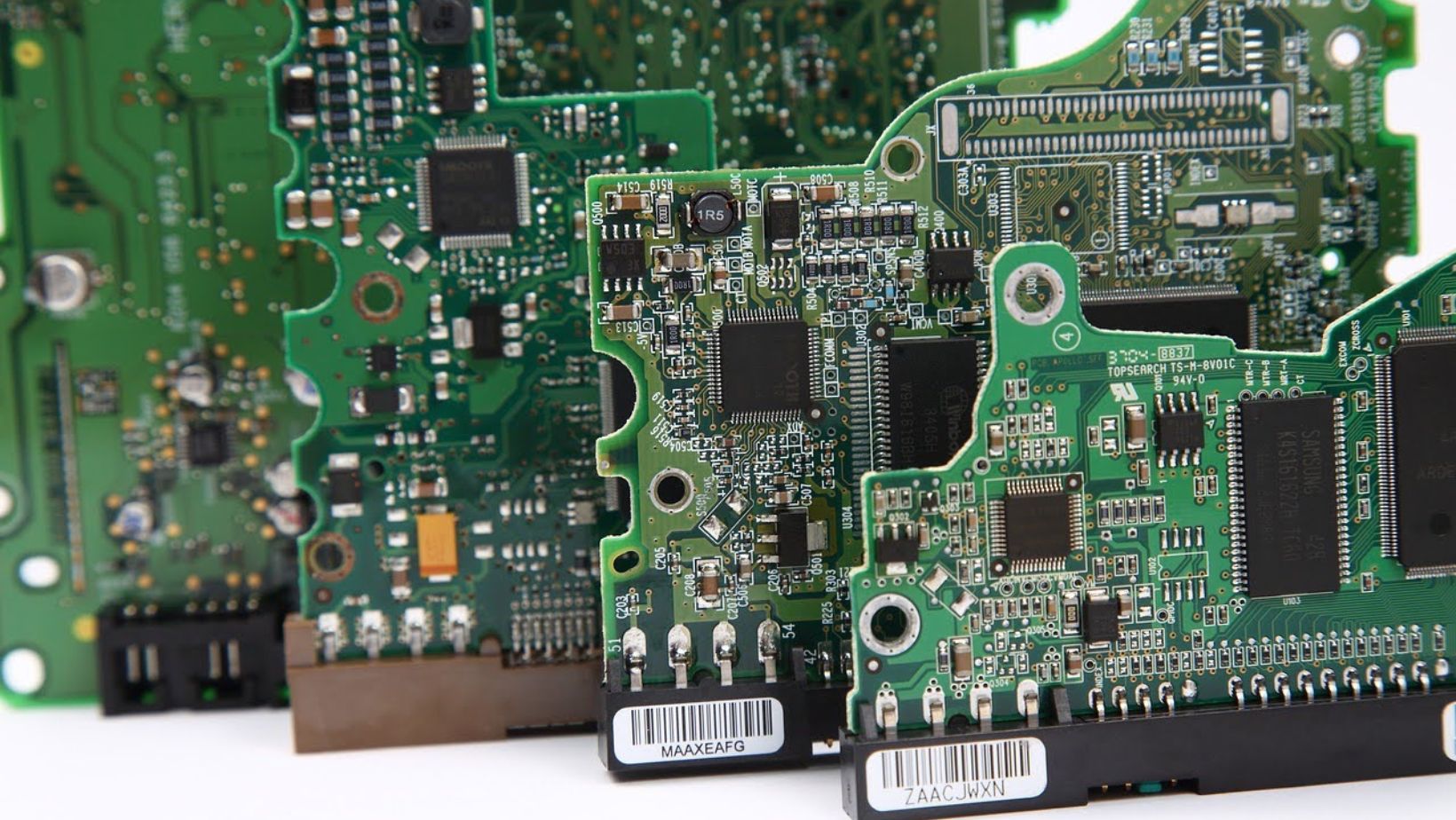
 Designing a printed circuit board (PCB) requires precision, attention to detail, and a thorough understanding of both electrical and mechanical constraints. Even small design mistakes can lead to performance issues, manufacturing delays, or costly rework. Understanding the most common PCB design mistakes and how to avoid them is key to ensuring your project’s success.
In this blog, we will explore the most frequent PCB design errors and provide tips on how to avoid them, leading to a smoother design-to-production process.
Importance of Avoiding PCB Design Mistakes
PCB design is the foundation of any electronic device, and even the smallest mistake can ripple through the entire development cycle. Whether you’re designing a simple consumer product or a complex industrial system, avoiding design errors can save time and money while improving product reliability.
One of the first steps in ensuring high-quality designs is working with a trusted manufacturer. Companies like OurPCB provide valuable insights into design considerations and offer tailored PCB solutions to help minimize errors from the start. Now, let’s dive into the common mistakes and how to prevent them.
Common PCB Design Mistakes and How to Avoid Them
Improper Trace Width and Spacing
One of the most frequent issues in PCB design is selecting incorrect trace widths or failing to maintain proper spacing between traces. If traces are too thin or too close to each other, it can lead to overheating, signal interference, or short circuits. This is especially problematic in high-current applications where traces need to carry more power.
How to avoid it:
- Calculate the appropriate trace width based on the current-carrying requirements using PCB trace calculators.
- Follow industry-standard trace width and spacing guidelines, such as those defined by IPC standards.
- Ensure sufficient spacing between high-voltage and low-voltage traces to prevent electrical arcing or interference.
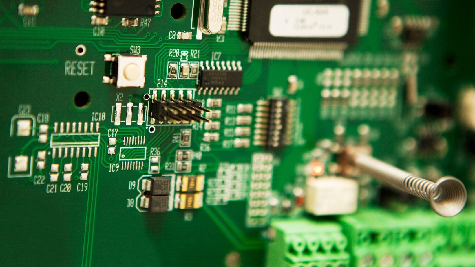
Incorrect Via Placement
Vias are crucial for connecting different layers in a multi-layer PCB. Incorrect via placement or using the wrong type of vias can lead to signal loss, power issues, or mechanical failure. For example, placing too many vias close together can weaken the structural integrity of the board, while using oversized vias unnecessarily reduces available board space.
How to avoid it:
- Use vias judiciously and place them where absolutely necessary.
- Select the right type of vias for your design, such as through-hole, blind, or buried vias, based on your specific needs.
- Avoid placing vias too close to the edges of components, as this can complicate soldering and assembly.
Poor Component Placement
Proper component placement is critical for both the electrical performance and manufacturability of your PCB. Poor placement can result in thermal issues, difficult routing, or problems during the assembly process. Components placed too close to the edge of the board or too close to each other can interfere with assembly, while components placed near heat-sensitive areas may degrade more quickly.
How to avoid it:
- Group components logically based on their function and signal flow to reduce unnecessary routing.
- Keep heat-sensitive components away from high-heat areas such as power supply circuits or high-current paths.
- Ensure adequate spacing between components to allow for efficient soldering, heat dissipation, and repairability.
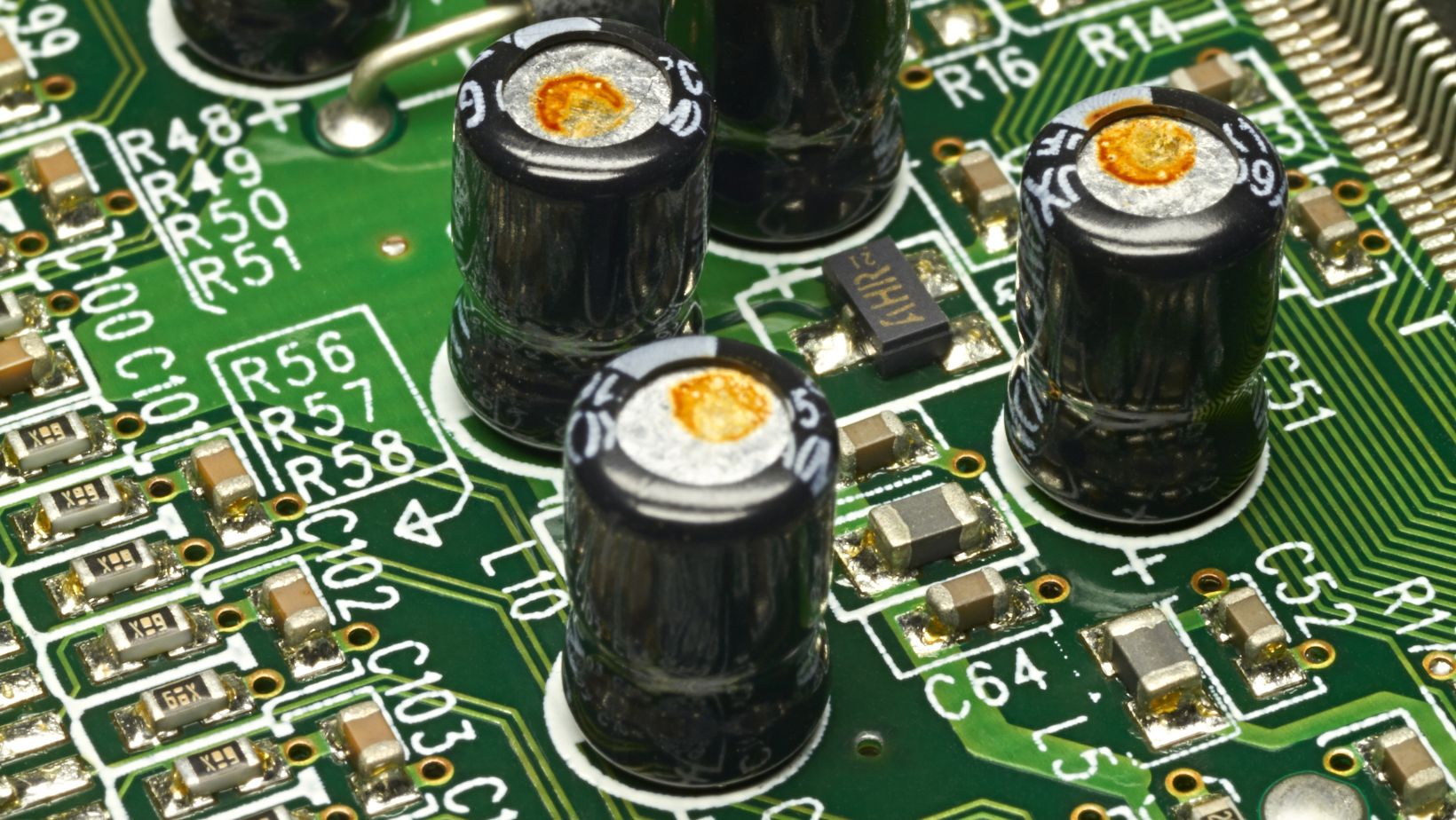
Insufficient Thermal Relief
When designing PCBs, especially for high-power applications, thermal management is essential. A common mistake is failing to account for proper heat dissipation, which can lead to overheating, damaged components, and reduced product lifespan. Without adequate thermal relief, soldering processes can also become difficult.
How to avoid it:
- Use thermal relief pads in the design to help dissipate heat away from critical components.
- Consider adding heat sinks or thermal vias to improve heat management for high-power areas.
- Utilize copper pours for ground and power planes to reduce thermal resistance.
Incorrect Grounding
A well-designed grounding system is crucial for ensuring signal integrity and preventing noise issues. One of the most common mistakes in PCB design is poor grounding, which can cause electromagnetic interference (EMI) and power noise. Splitting ground planes unnecessarily or failing to provide a low-impedance path for current flow are frequent errors.
How to avoid it:
- Use a single, continuous ground plane when possible to minimize impedance and reduce noise.
- For multi-layer PCBs, place the ground plane directly under the signal layers to shield against EMI.
- Avoid creating “ground loops” by ensuring that all ground paths are routed to a single point.
Neglecting Design for Manufacturability (DFM)
Designing a PCB that works in simulation is one thing, but designing one that can be reliably manufactured is another. Failing to consider Design for Manufacturability (DFM) can lead to issues during the production stage, such as component placement conflicts, difficulty with soldering, or misalignment of layers.
How to avoid it:
- Work closely with your PCB manufacturer during the design phase to ensure your design meets their fabrication capabilities.
- Follow DFM guidelines to avoid design features that are difficult or expensive to manufacture, such as non-standard hole sizes, overly tight tolerances, or complex routing paths.
- Ensure that the board’s layout accounts for automated assembly processes, such as pick-and-place machines and reflow ovens.
Ideal Practices for a Reliable PCB Design
To avoid the most common design mistakes and ensure that your PCB is both functional and manufacturable, it’s essential to follow some best practices throughout the design process. Here are some key strategies:
Conduct a Thorough Design Overview
Before sending your design off for fabrication, perform a thorough design review. This includes checking all electrical connections, ensuring that trace widths and spacing comply with standards, and verifying component placement and orientation. Consider using design rule checking (DRC) software to automate part of the review process.
Simulate the Circuit
Simulating your PCB design before fabrication helps identify potential electrical issues early on. Circuit simulation software allows you to test for problems like signal integrity, crosstalk, and power distribution issues. Simulations are especially important for high-frequency designs, where even minor errors can have significant impacts.
Utilize Design for Testability (DFT)
Designing your PCB with testing in mind can make it easier to identify and resolve issues during production. Include test points in your design so that each circuit can be easily probed and tested for continuity, functionality, and performance during manufacturing. This reduces the risk of delivering defective boards.
The Role of Advanced Tools in PCB Design
Advanced PCB design tools have become essential for minimizing errors and improving the overall quality of a design. Modern design software provides features such as automatic routing, real-time design rule checking, and multi-layer support, which help engineers avoid common mistakes during the design process.
Design Rule Checking (DRC): DRC ensures that your design adheres to specified rules, such as trace width, spacing, and component clearance, preventing simple but costly mistakes.
Signal Integrity Tools: These tools allow you to simulate how electrical signals will behave on the PCB, helping to avoid issues such as reflection, ringing, and crosstalk.
Thermal Analysis: Simulating heat distribution across the PCB can prevent thermal failures in the final product by identifying areas where excessive heat might build up.
Conclusion
PCB design is a complex process that requires careful attention to detail and an understanding of both electrical and mechanical considerations. By avoiding common design mistakes such as improper trace widths, poor component placement, and insufficient thermal relief, you can ensure that your board will perform reliably and be easier to manufacture. Working with a trusted partner like OurPCB can further reduce the risk of errors and help guide you through the process, from design to final production.